

Having worked in the photonics industry before joining the patent profession, I have some appreciation of the long-standing challenges associated with the manufacture of photonic integrated circuits (PICs) for applications such as high-speed optical communications, optical signal processing, optical sensing, and quantum information processing. I was therefore intrigued to read this article discussing the use of photonic wire bonding for the hybrid integration of photonic components which are formed on different substrates, and then mounted on a common carrier e.g. for the hybrid integration of III-V semiconductor laser chips with photonic components such as silicon photonics circuits and passive planar lightwave circuits. Photonic wire bonding relies upon the use of two-photon polymerisation of a photoresist material to create optical waveguide interconnects along arbitrary paths in three dimensions between photonic components. Although photonic wire bonding would appear to have been in development since at least 2011, it will be interesting to see whether photonic wire bonding is adopted more widely for the automated mass-manufacture of PICs in the future.
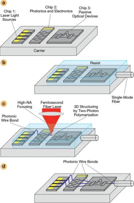
Photonic wire bonds maintain the performance and versatility
advantages of hybrid integration approaches while offering a path
toward highly scalable automated mass production.
www.photonicsspectra-digital.com/...
The content of this article is intended to provide a general guide to the subject matter. Specialist advice should be sought about your specific circumstances.
